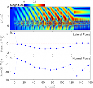
Metasurface for Laser Sail Applications: Laser sails are a proposed type of spacecraft –propelled by a high-power laser– that can potentially reach relativistic speeds. Such a scheme, however, faces many challenges, and among those are the strict limitations on the sail’s mass, density, and absorptivity, as well as the ability of the sail to self-stabilize within the beam. Our research is focused on developing a thin dielectric optical metasurface as a self-stabilizing, non-absorptive laser sail. A metasurface is a material that has its optical properties dramatically altered by structuring the material on the sub-wavelength scale. The reflection and refraction of the light is controlled by engineering the local, microscopic scattering properties and arbitrary optical wave-fronts can be engineered. This local control can be used as a means of passive orientation correction and positioning of laser sails, with the deflected light imparting both forward and lateral forces selectively on various parts of the sail.

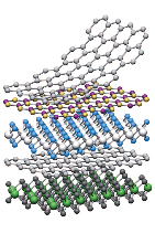
Van der Waals Heterostructures for STM: Van der Waals (vdW) heterostructures are stacks of two-dimensional crystals. An example material is bilayer graphene (BLG), which, like other 2D crystals, has a melting temperature that decreases with thickness. Stacking BLG on thin hexagonal boron nitride (hBN) provides a cleaner electronic environment than BLG place on SiO2 substrates. Devices, such as tunable transistors and optical instruments with tunable absorption properties, can be made from 2D heterostructures. Studying these stacks using STM allows us to probe devices with excellent spatial and energetic resolutions. The goal of our STM measurements on BLG is to demonstrate the best possible understanding of the underlying electronic structure and to further inform our understanding of the physics of vdW heterostructures. However, local probes, such as STM, are invasive, and the tip acts as a top gate so that both band structure and doping change with the voltage probed. By extending earlier work on optics and transport measurements to the STM we will be able to look for new physics.
STM Optical Experiments
TBA
Imaging Viscous Transport in Graphene
Using the versatility of a STM we generate and probe tunable quantum dots (QD) in monolayer graphene (MLG)/hexagonal boron nitride (hBN) heterostructures. These electrostatically-defined QDs serve as local scatterers for MLG charge carriers under transport conditions. We use a STM technique known as scanning tunneling potentiometers (STP) to map the local electrochemical potential around these local scattering sources with an applied source-drain current. In doing so, we probe the nature and onset of strongly-correlated electronic behavior that leads to viscous carrier flow in MLG.

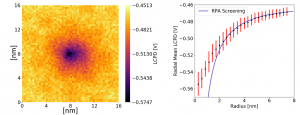
Screening in 2D Van Der Waals Materials: Charge interactions in atomically thin materials can be much stronger than in their 3D counterparts. These interactions lead to novel many-body phenomena, as well as strong excitonic effects. We develop local probe methods that can be used to directly measure the strength of those interactions by analyzing the how charge impurities perturb the local potential in 2D materials.
Josephson Junction STM: The central challenge qubits are currently facing is unavoidable environmental noise that leads to quantum decoherence. However, we do not currently have a diagnostic tool to directly probe the source of this noise. Our lab is working towards developing a new type of scanned probe method that combines the novel, quantum mechanical properties of Josephson junctions with the spatial resolution of scanning tunneling microscopy/spectroscopy (STM/STS) enables the energy spectrum of a surface to be probed with sub-nm spatial resolution and ~ GHz energy resolution.

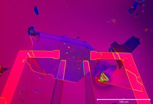
Coulomb Drag: By placing two sheets of conducting material close to each other with a thin insulating spacer, a system that favors highly correlated charge carriers can be created. These types of systems promote behavior that, under the right conditions, lead to a “Coulomb drag” mechanism where current through a ‘drive’ layer is able to induce a voltage across a second ‘drag’ layer due to interlayer electron-electron scattering leading to momentum and energy transferral. Using mono or bilayer graphene as our conducting sheets, and hexagonal boron nitride as our insulating spacer, we are able to tune carrier density and perform a wide range of transport measurements. When strong magnetic fields are applied to the system, such structures are theorized to host exotic states known as an exciton condensate.