University of Wisconsin–Madison
UW Crest

Victor Brar Lab

  • Home
  • Research
  • Publications
  • Contact
  • Team
    Log in

The Brar Lab at the University of Wisconsin--Madison

Sail thermal runaway

A simulation of a Si/SiO2 laser sail vaporizing under intense laser illumination.

1 degree light steerer

Gaussian beam incident on a highly reflective laser sail (1 degree steerer). Light is reflected 1 degree.

"UW" with CO on Cu(111)

"UW" lettering made by rearranging adsorbed CO molecules on Cu(111). Note the "sea of electrons" surrounding the letters.

Circle of CO on Cu(111)

Carbon monoxide molecules arranged into a "quantum corral" on Cu(111) using the lab's scanning tunneling microscope (STM).

dI/dV maps: CO on Cu(111)

Left image: Density of electron states (DOS) map taken at 380 mV. Right image: DOS map of the same area at an energy of 190 mV .

Bilayer graphene (BLG)

Atomically resolved image of BLG. Individual carbon atoms exhibit a well-known honeycomb lattice.

STM

Our scanning tunneling microscope (STM) is used to image surfaces at the atomic level through quantum tunneling of electrons.

STM Head

The head of our STM where the scanning tip is located. The tip is made from an atomically-sharp wire.

Thermal Emitter

These metasurfaces can have angular and near-field profiles that differ significantly from traditional blackbodies.

Learn more

Charged Defect Screening

Charged defect in a MLG/hBN system. STM topography (left) and KPFM image (right) showing the local potential variation.

WELCOME TO THE BRAR LAB!

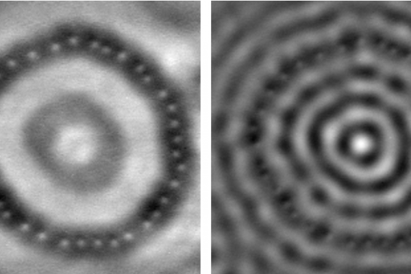
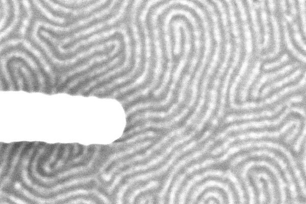
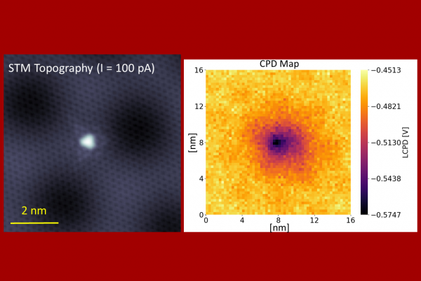
We probe the electronic, magnetic, and optical behavior of materials at the atomic-scale in search of new phenomena that have both fundamental and technological importance. Examples of such effects include highly localized plasmonic modes, long-range magnetic interactions, and deep impurity states. The types of behavior we search for are general and manifest in many types of systems, but they often occur most dramatically in exotic materials that exhibit quantum effects and in low dimensional materials with strong electron interactions. When new behavior is discovered locally, we use large-scale lithographic methods to structure the host material, such that those phenomena can manifest macroscopically in ways that can be utilized for new device applications.

Site footer content

University logo that links to main university website Part of the Universities of Wisconsin

Home

  • Home
  • Research
  • Publications
  • Contact
  • Team

Contact Us

  • office: 5332 Chamberlin Hall
    lab: 1246 Chamberlin Hall
  • Map map marker
  • Email: vbrar@wisc.edu
  • Phone: 608-262-1139
    • linkedin

Website feedback, questions or accessibility issues: brown56@wisc.edu.

Learn more about accessibility at UW–Madison.

This site was built using the UW Theme | Privacy Notice | © 2025 Board of Regents of the University of Wisconsin System.